The 555 timer IC is an integrated circuit (chip) used in a variety of timer, delay, pulse generation, and oscillator applications. Derivatives provide two (556) or four (558) timing circuits in one package.[2] It was commercialized in 1972 by Signetics.[3][4] Numerous companies have made the original bipolar timers and similar low-power CMOS timers too. In 2017, it was said over a billion 555 timers are produced annually by some estimates, and "probably the most popular integrated circuit ever made."[5]


History

The timer IC was designed in 1971 by Hans Camenzind under contract to Signetics.[3] In 1968, he was hired by Signetics to develop a phase-locked loop (PLL) IC. He designed an oscillator for PLLs such that the frequency did not depend on the power supply voltage or temperature. Signetics subsequently laid off half of its employees due to the 1970 recession, and development on the PLL was thus frozen.[6] Camenzind proposed the development of a universal circuit based on the oscillator for PLLs and asked that he develop it alone, borrowing equipment from Signetics instead of having his pay cut in half. Camenzind's idea was originally rejected, since other engineers argued the product could be built from existing parts sold by the company; however, the marketing manager approved the idea.[7]
The first design for the 555 was reviewed in the summer of 1971. Assessed to be without error, it proceeded to layout design. A few days later, Camenzind got the idea of using a direct resistance instead of a constant current source finding later that it worked. The change decreased the required 9 pins to 8 so the IC could be fit in an 8-pin package instead of a 14-pin package. This revised design passed a second design review with the prototypes completed in October 1971 as the NE555V (plastic DIP) and SE555T (metal TO-5).[8] The 9-pin copy had been already released by another company founded by an engineer who attended the first review and retired from Signetics; that firm withdrew its version soon after the 555 was released. The 555 timer was manufactured by 12 companies in 1972 and it became a best selling product.[6]
Name
Several books report the name 555 comes from the three 5 kilohm resistors inside the chip.[9][10][11] However, in a recorded interview with an online transistor museum curator,[12] Hans Camenzind said "It was just arbitrarily chosen. It was Art Fury (Marketing Manager) who thought the circuit was gonna sell big who picked the name '555'."[13]
Design
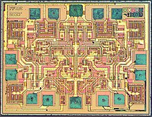
Depending on the manufacturer, the standard 555 package includes 25 transistors, 2 diodes and 15 resistors on a silicon chip installed in an 8-pin dual in-line package (DIP-8).[14] Variants available include the 556 (a DIP-14 combining two complete 555s on one chip),[15] and 558 / 559 (both a DIP-16 combining four reduced-functionality timers on one chip).[2]
The NE555 parts were commercial temperature range, 0 °C to +70 °C, and the SE555 part number designated the military temperature range, −55 °C to +125 °C. These were available in both high-reliability metal can (T package) and inexpensive epoxy plastic (V package) packages. Thus the full part numbers were NE555V, NE555T, SE555V, and SE555T.
Low-power CMOS versions of the 555 are also available, such as the Intersil ICM7555 and Texas Instruments LMC555, TLC555, TLC551.[16][17] [18][19] CMOS timers use significantly less power than bipolar timers; CMOS timers also cause less supply noise than bipolar version when the output switches states.[citation needed]
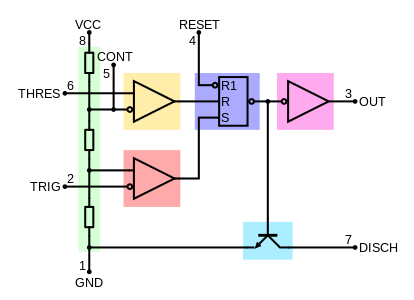
Internal schematic
The internal block diagram and schematic of the 555 timer are highlighted with the same color across all three drawings to clarify how the chip is implemented:[2]
- Green: Between the positive supply voltage VCC and the ground GND is a voltage divider consisting of three identical resistors, which create two reference voltages at 1⁄3 VCC and 2⁄3 VCC. The latter is connected to the "Control" pin. All three resistors have the same resistance, 5 kΩ for bipolar timers, 100 kΩ (or higher) for CMOS timers.
- Yellow: The comparator negative input is connected to the higher-reference voltage divider of 2⁄3 VCC (and "Control" pin), and comparator positive input is connected to the "Threshold" pin.
- Red: The comparator positive input is connected to the lower reference voltage divider of 1⁄3 VCC, and comparator negative input is connected to the "Trigger" pin.
- Purple: An SR flip-flop stores the state of the timer and is controlled by the two comparators. The "Reset" pin overrides the other two inputs, thus the flip-flop (and therefore the entire timer) can be reset at any time.
- Pink: The output of the flip-flop is followed by an output stage with push-pull (P.P.) output drivers that can load the "Output" pin with up to 200 mA for bipolar timers, lower for CMOS timers.
- Cyan: Also, the output of the flip-flop turns on a transistor that connects the "Discharge" pin to the ground.


Pinout
The pinout of the 8-pin 555 timer[1] and 14-pin 556 dual timer[20] are shown in the following table. Since the 556 is conceptually two 555 timers that share power pins, the pin numbers for each half is split across two columns.[2]
In the following table, longer pin names are used, because manufacturers never standardized the abbreviated pin names across all datasheets.

Modes
The 555 IC has the following operating modes:
- Astable (free-running) mode – the 555 can operate as an electronic oscillator. Uses include LED and lamp flashers, pulse generation, logic clocks, tone generation, security alarms, pulse position modulation and so on. The 555 can be used as a simple ADC, converting an analog value to a pulse length (e.g., selecting a thermistor as timing resistor allows the use of the 555 in a temperature sensor and the period of the output pulse is determined by the temperature). The use of a microprocessor-based circuit can then convert the pulse period to temperature, linearize it and even provide calibration means.
- Monostable (one-shot) mode – in this mode, the 555 functions as a "one-shot" pulse generator. Applications include timers, missing pulse detection, bounce-free switches, touch switches, frequency divider, capacitance measurement, pulse-width modulation (PWM), and so on.
- Bistable (flip-flop) mode – the 555 operates as a SR flip-flop. Uses include bounce-free latched switches.
- Schmitt Trigger (inverter) mode - the 555 operates as a Schmitt trigger inverter gate which converts a noisy input into a clean digital output.
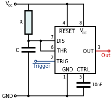
Astable


In the astable configuration, the 555 timer puts out a continuous stream of rectangular pulses having a specific frequency. The astable configuration is implemented using two resistors, 


In the first pulse, the capacitor charges from zero to two-thirds of the supply voltage, however, in later pulses, it only charges from one-third to two-thirds of the supply voltage. Consequently, the first pulse has a longer high time interval compared to later pulses. Moreover, the capacitor charges through both resistors but only discharges through
The high time interval of each pulse is given by:

The low time interval of each pulse is given by:

Hence, the frequency 
[24]
and the duty cycle (%) is given by:

where 


Resistor
power capability of
, per Ohm's law.
- Particularly with bipolar 555s, low values of
The first cycle will take appreciably longer than the calculated time, as the capacitor must charge from 0 V to 2⁄3 of VCC from power-up, but only from 1⁄3 of VCC to 2⁄3 of VCC on subsequent cycles.
Shorter duty cycle
To create an output high time shorter than the low time (i.e., a duty cycle less than 50%) a fast diode (i.e. 1N4148 signal diode) can be placed in parallel with R2, with the cathode on the capacitor side. This bypasses R2 during the high part of the cycle so that the high interval depends only on R1 and C, with an adjustment based the voltage drop across the diode. The voltage drop across the diode slows charging on the capacitor so that the high time is longer than the expected and often-cited ln(2)*R1C = 0.693 R1C. The low time will be the same as above, 0.693 R2C. With the bypass diode, the high time is

where Vdiode is when the diode's "on" current is 1⁄2 of Vcc/R1 which can be determined from its datasheet or by testing. As an extreme example, when Vcc = 5 V and Vdiode= 0.7 V, high time = 1.00 R1C which is 45% longer than the "expected" 0.693 R1C. At the other extreme, when Vcc= 15 V and Vdiode= 0.3 V, the high time = 0.725 R1C which is closer to the expected 0.693 R1C. The equation reduces to the expected 0.693 R1C if Vdiode = 0 V.
Monostable
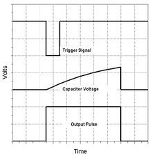
In monostable mode, the output pulse ends when the voltage on the capacitor equals 2⁄3 of the supply voltage. The output pulse width can be lengthened or shortened to the need of the specific application by adjusting the values of R and C.[25]
The output pulse is of width t, which is the time it takes to charge C to 2⁄3 of the supply voltage. It is given by

where 
While using the timer IC in monostable mode, the time span between any two triggering pulses must be greater than the RC time constant.[26]
Bistable
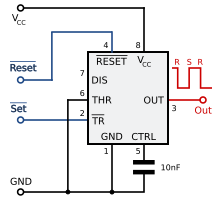

In bistable mode, the 555 timer acts as an SR flip-flop. The trigger and reset inputs are held high via pull-up resistors while the threshold input is grounded. Thus configured, pulling the trigger momentarily to ground acts as a 'set' and transitions the output pin to VCC (high state). Pulling the reset input to ground acts as a 'reset' and transitions the output pin to ground (low state). No timing capacitors are required in a bistable configuration. The discharge pin is left unconnected, or may be used as an open-collector output.[27]
Schmitt trigger


A 555 timer can be used to create a Schmitt trigger inverter gate which converts a noisy input into a clean digital output. The input signal should be connected through a series capacitor which then connects to the trigger and threshold pins. A resistor divider, from VCC to GND, is connected to the previous tied pins. The reset pin is tied to VCC.
Packages

In 1972, Signetics originally released the 555 timer in DIP-8 and TO5-8 metal can packages, and the 556 timer was released in DIP-14 package.[4]
In 2012, the 555 was available in through-hole packages as DIP-8 (2.54 mm pitch),[28] and surface-mount packages as SO-8 (1.27 mm pitch), SSOP-8 / TSSOP-8 / VSSOP-8 (0.65 mm pitch), BGA (0.5 mm pitch).[1]
In 2006, the dual 556 timer was available in through-hole packages as DIP-14 (2.54 mm pitch),[20] and surface-mount packages as SO-14 (1.27 mm pitch) and SSOP-14 (0.65 mm pitch).
The MIC1555 is a CMOS 555-type timer with three fewer pins available in SOT23-5 (0.95 mm pitch) surface-mount package.[29]
Specifications

These specifications apply to bipolar NE555. Other 555 timers can have different specifications depending on the grade (industrial, military, medical, etc.).
Derivatives
Numerous companies have manufactured one or more variants of the 555, 556, 558 timers over the past decades as many different part numbers. The following is a partial list:
- Table notes
- All information in the above table was pulled from references in the datasheet column, except where denoted below.
- For the "Timer Total" column, a "*" denotes parts that are missing 555 timer features.
- For "Iq" column, a 5 volt supply was chosen as a common voltage to make it easier to compare. The value for Signetics NE558 is an estimate because NE558 datasheets don't state Iq at 5V.[2] The value listed in this table was estimated by comparing the 5V to 15V ratio of other bipolar datasheets, then derating the 15V parameter for the NE558 part, which is denoted by the "*".
- For the "Frequency Max" column, a "*" denotes values that may not be the actual maximum frequency limit of the part. The MIC1555 datasheet discusses limitations from 1 to 5 MHz.[29] Though most bipolar timers don't state the maximum frequency in their datasheets, they all have a maximum frequency limitation of hundreds of kHz across their full temperature range. Section 8.1 of the Texas Instruments NE555 datasheet[1] states a value of 100 kHz, and their website shows a value of 100 kHz in timer comparison tables. In Signetics App Note 170, states that most devices will oscillate up to 1 MHz, however when considering temperature stability it should be limited to about 500 kHz.[2] The application note from HFO mentions that at higher supply voltages the maximum power dissipation of the circuit might limit the operating frequency, as the supply current increases with frequency.[41]
- For the "Manufacturer" column, the following associates historical 555 timer manufacturers to current company names.
- Fairchild Semiconductor was sold to ON Semiconductor in 2016.[42] ON Semiconductor was founded in 1999 as a spinoff of Motorola Semiconductor Components Group.[43] The MC1455 started as a Motorola product.
- Intersil was sold to Renesas Electronics in 2017.[44] The ICM7555 and ICM7556 started as Intersil products.
- Micrel was sold to Microchip Technology in 2015.[45] The MIC1555 started as a Micrel product.
- National Semiconductor was sold to Texas Instruments in 2011.[46] The LM555 and LM556 started as a National Semiconductor products.
- Signetics was sold to Philips Semiconductor in 1975, later to NXP Semiconductors in 2006.[47]
- Zetex Semiconductors was sold to Diodes Incorporated in 2008.[48] The ZSCT1555 started as a Zetex product.
556 dual timer

The dual version is called 556. It features two complete 555 timers in a 14 pin package; only the two power supply pins are shared between the two timers.[20][15] In 2020, the bipolar version was available as the NE556,[20] and the CMOS versions were available as the Intersil ICM7556 and Texas Instruments TLC556 and TLC552. See derivatives table in this article.[16][39][38]
558 quad timer

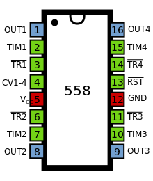

The quad version is called 558 that has four reduced-functionality timers in a 16 pin package designed primarily for "monostable multivibrator" applications.[49][2] By 2014, many versions of 16-pin NE558 have become obsolete.[50]
Partial list of differences between 558 and 555 chips:[2][50]
- One VCC and one GND, similar to 556 chip.
- Four "Reset" are tied together internally to one external pin (558).
- Four "Control Voltage" are tied together internally to one external pin (558).
- Four "Triggers" are falling-edge sensitive (558), instead of level sensitive (555).
- Two resistors in the voltage divider (558), instead of three resistors (555).
- One comparator (558), instead of two comparators (555).
- Four "Output" are open-collector (O.C.) type (558), instead of push-pull (P.P.) type (555). Since the 558 outputs are open-collector, pull-up resistors are required to "pull up" the output to the positive voltage rail when the output is in a high state. This means the high state only sources a small amount of current through the pull-up resistor.
| This article uses material from the Wikipedia article Metasyntactic variable, which is released under the Creative Commons Attribution-ShareAlike 3.0 Unported License. |